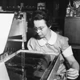
U.S. patent 2,597,562, “Electrically Conducting Layer,” is issued to Katharine Burr Blodgett for conductive thin-film coatings.
On May 20, 1952, Katharine Burr Blodgett was issued U.S. patent 2,597,562 for an “Electrically Conducting Layer.” This invention described methods for forming thin, electrically conductive coatings on substrates, linking her expertise in films and surfaces to emerging needs in electronics and instrumentation.
The patent detailed how particular materials and deposition techniques could yield layers that combined electrical conductivity with the optical or mechanical properties of underlying surfaces. Such coated layers were relevant for sensors, display devices, and components where electrical pathways had to be integrated unobtrusively into structural or optical elements.
This event illustrates Blodgett’s continuing role in advancing thin‑film applications beyond optics into electrical functionality. As industry moved toward miniaturization and the integration of electrical properties into diverse materials, her research contributed to enabling technologies that prefigured later developments in microelectronics and functional coatings. The patent also highlights her sustained inventive output in the 1950s, showing that she remained an active contributor to GE’s portfolio of intellectual property at a time when women scientists in corporate labs were still exceedingly rare.