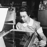
U.S. patent 2,636,832, “Method of Forming Semiconducting Layers on Glass and Article Formed Thereby,” is issued to Katharine Burr Blodgett.
On April 28, 1953, Katharine Burr Blodgett was granted U.S. patent 2,636,832 for a “Method of Forming Semiconducting Layers on Glass and Article Formed Thereby.” This invention described how to deposit semiconducting films onto glass substrates, creating composite materials with both optical transparency and electronic properties.
Blodgett’s method involved carefully controlled chemical and thermal processes to achieve uniform semiconducting layers, addressing challenges of adhesion, stability, and performance. The resulting coated glass could serve in devices where electronic behavior needed to be integrated into transparent or insulating structures, anticipating future uses in photoelectric cells and sensor technologies.
This patent is historically significant for its link between thin‑film surface chemistry and semiconductor technology. At a time when semiconductor physics was rapidly advancing, Blodgett’s work pointed toward applications in which glass and electronic materials would be combined, foreshadowing modern efforts in display technology and solar energy. For women’s‑history research, the patent exemplifies her position at the intersection of multiple cutting‑edge domains—optics, electronics, and materials science—while she remained one of the very few women credited as an inventor in these fields within a major industrial laboratory.